

Sakshi Education
- Power diodes are uncontrolled devices. In other words their turn on and turn off characteristics are not under control. Power transistors, however, posses control characteristics. These are turned on when a current signal is given to base or control terminal.
- The transistor remains in the on state so long as control signal is present. When this control signal is removed, a power transistor is turned off.
- Power transistors are of three types as under
- BJTSs
- MOSFETs
- IGBTs
Power BJT
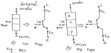
- Biploar transistor is a three layer, two junction npn or pnp semiconductor device with one p-region sandwitched by two n- regions, fig (a), npn transistor is obtained. With two p-regions sandwitching one n-region, fig (b), pnp transistor is obtained.
- The term bipolar denotes that the current flow in the device due to the movement of both holes and electrons.
- A BJT has 3 termianls named collector, emitter and base. An emitter is indicated an arrow head indicating the direction of emitter current. No arrow is associated with base or collector.
- Fully controlled device means both ON & OFF states are controlled.
Steady State Characteristics:
Out of these possible circuit configurations for a transistor, common emitter arrangement is more common in switching applications. So npn transistors will only be considered.
Input Characteristics:
A graph between base current IB and base emitter voltage VBE gives input characteristics
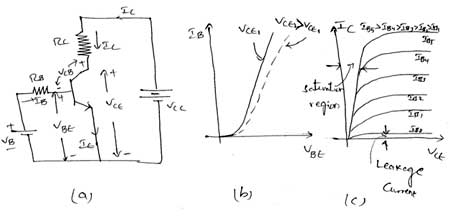
Fig (a) npn transistor circuit characteristics
Fig (b) Input characteristics
Fig (c) Output characteristics
- Cut off region for OFF state
- Saturation region for On state
Features:
- Current controlled device
- The ON state voltage drop of BJT is less and its associated with losses are less.
- Switching power loss is high
- Input impedance of BJT is low
- Negative temp. co-efficient effect
- Secondary breakdown occurs
- Parallel operation is not possible
Safe Operating Area (SOA) of Power Transistor:
- The SOA of a power transistor specifies the safe operating limits of collector current IC versus collector emitter voltage VCE.
- For reliable operation of the transistor, the collector current and voltage must always lie within the area.
- Actually, FB SOA and RB SOA are the two types of SOA specified by the manufacturers.
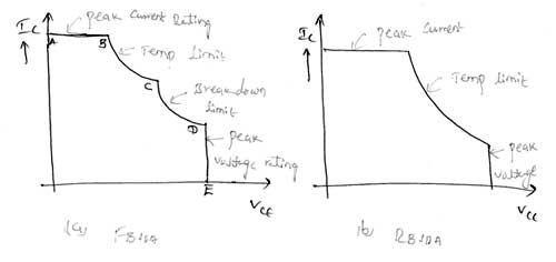
- During turn-off, a transistor is subjected to high current and high voltage with base emitter junction reverse biased.
Power MOSFET
- MOSFET is a modern electronic device developed by combining areas of field effect concept and MOS technology.
- BJT is a current controlled device whereas a power MOSFET is a voltage controlled device. As its operation depends upon the flow of majority carriers only. MOSFET is a unipolar device.
- The control signal or base current in BJT is much larger than the control signal (or gate current) required in a MOSFET.
- Power MOSFETs are of two types:
- n-channel enhancement MOSFET
- p-channel enhancement MOSFET
- Out of these two types, n-channel enhancement MOSFET is more common because of higher mobility of electrons.
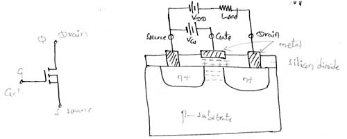
- Whan gate circuit is open, no current flows from drain to source and load because of one reverse biased n+- p junction.
- When gate is made positive with respect to source an electric field is established as shown in fig. Eventually, induced negative charges in the p – substrate below SiO2 layer are formed, these negative charges called electrons, from n-channel and current can flow from drain to source as shown by the arrow.
- If VGS is made positive, n-channel becomes more deep and therefore more current flows from D to S. This shows that drain current ID is enhanced by the gradual increase of gate voltage, hence the name enhancement MOSFET.
- A power MOSFETs actually consists of a parallel connection of thousands of basic MOSFET cells on the same single chip of silicon.
- Power MOSFET conduction is due to majority carriers. Therefore, time delays caused by removal or recombination of minority carriers are eliminated. Thus, power MOSFET can work at switching frequencies in the megahertz range.
MOSFET Characteristics:
a) Transfer Characteristics: This characteristics shows the variation of drain current ID as a function of gate source voltage VGS.
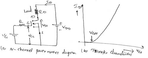
- It is seen that there is threshold voltage VGST below which the device is OFF. The magnitude of VGST is of the order of 2 to 3V.
b) Ouput Characteristics: This characteristics shows the variation of drain current ID as a function of drain source voltage VDS.
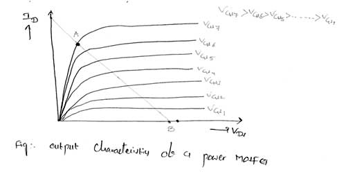
- For low value of VDS the graph between ID - VDS is almost linear, this indicates a constant value of on-resistance RDS = VDS/ ID
- For given VGS, if VDS is increased output characteristics is relatively flat indicating that drain current is nearly constant.
- A local line intersects the output characteristics at A and B. Here A indicates fully ON condition and B fully OFF state. Power MOSFET a operates as a switch either at A or B just like a BJT.
Comparision of MOSFET and BJT
MOSFET
- Power MOSFET has lower switching losses but its ON resistance and conduction losses are more. So at high frequency applications power MOSFET is the obvious choice.
- MOSFET is a voltage controlled device.
- MOSFET has positive temperature co-efficient for resistance, this makes parallel operation of MOSFETs easy. If a MOSFET shares increased current initially, it heats up faster, its resistance rises and this increased resistance causes this current to shift to other devices in parallel.
- A BJT has higher switching losses but lower conduction loss. It lower operating frequencies (less than 10Hz to 30 KHz). BJT is superior.
- BJT is current controlled device.
- A BJT has negative temperature co-efficient for resistance, so current sharing resistors are necessary during parallel operation of BJT.
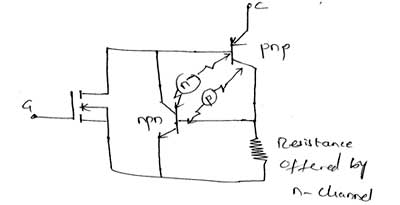
IGBT (Insulated-Gate Bipolar Transistor)
- IGBT is a new development in the area of power MOSFET technology. This device combines into it the advantage of both MOSFET and BJT.
- IGBT has high input impedance like a MOSFET and low ON state power loss as in a BJT. Further, IGBT is free from second breakdown problem present in BJT.
- IGBT is also called as metal oxide insulated gate transistor (MOSIGT).
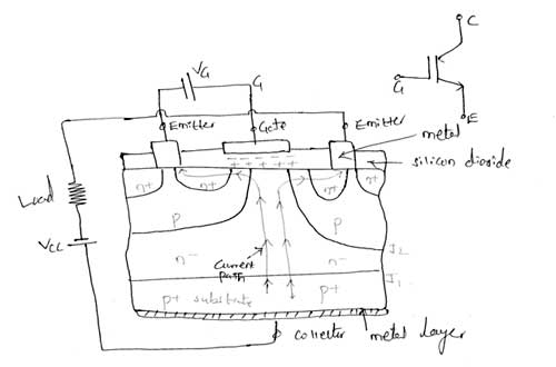
- It is constructed virtually in the same manner as a power MOSFET. There is however, a major difference in the substrate.
- The n+ layer substrate at the drain in a power MOSFET is now substituted in the IGBT by a p+ layer sustrate called collector.
- When gate is positive with respect to emitter and with gate emitter voltage more than the threshold voltage of IGBT, an n-channel is formed in the p-region as in a power MOSFET. This n-channel short circuits the n-region with n+ emitter regions.
- An electron movement in the n-channel in turn causes substantial hole injection from p+ substrate layer into the epitaxial n- layer. Eventually, a forward current is established.
- The 3 layers p+, n- and p constitutes a pnp transistor with p+ as emitter, n- as base and p as collector. Also n-, p and n+ layers constitute npn transistor. Here n- serves as base for pnp transistor and also as collector for npn transistor.
- Further, p serves as collector for pnp device and also as base for npn transistor.
IGBT Characteristics:
- This characteristics shows the plot of collector current IC versus collector emitter voltage VCE for various values of gate emitter voltages.
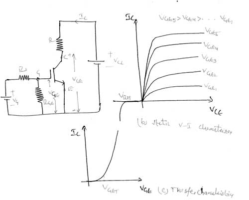
- In forward direction, the shape of the output characteristics is similar to that of BJT. But here the controlling parameter is gate-emitter voltage VGE because IGBT is a voltage controlled device.
- Transfer characteristics is similar to that of power MOSFET.
Applications:
- IGBTs are widely used in medium power applications such as dc and ac motor drives, UPS systems, power supplies and drives for solenoids, relays and contactors.
- Though IGBTs are somewhat more expensive than BJTs, yet they are becoming popular because of lower gate drive resistance, lower switching losses and smaller snubber circuit requirements.
- IGBTs are more efficient with less size as well as cost, as compared to converters based on BJTs.
- Ratings upto 1200V, 500A.
Published date : 13 Apr 2016 10:28AM